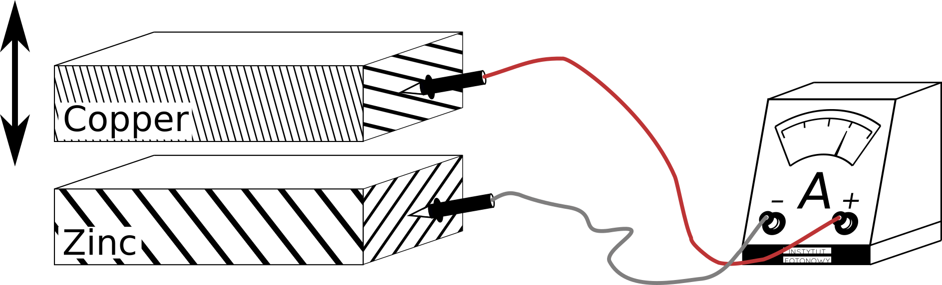
Before one can firmly answer such a question lets first define the Work Function (WF) and the Contact Potential Difference (CPD).
Let’s start with the notion of work function since it is commonly misunderstood. The meaning of WF evolved over time, and some people missed the change.
Work function
Definition
The definition of work function is that it is a minimum energy necessary to remove an electron from the bulk of a material through a given surface provided the surface is uncharged.
A common representation of the WF as the energy difference between the lowest vacuum state and the Fermi level of the material is often incorrect. One needs to keep in mind that the surface must be void of any excess charge!
Tungsten work functions
During development of electron microscopy, it has been discovered in 1936 that a single tungsten crystal shows anisotropic emission of electrons when heated.
Some crystallographic faces of tungsten emitted electrons only at very high temperatures of 2000 K while others were active even at 700 K.
It may come as a surprise since the Fermi level for a given crystal in equilibrium is uniform across the crystal and so is the energy difference between the lowest vacuum level and the most energetic electrons within the metal. So, should be the work function defined as the difference!
Yet electrons poured out easier in some directions than in others.
Namely, work function depended on the surface orientation with respect to the crystal lattice.
A Tungsten monocrystal has a single Fermi level, there is only one lowest vacuum level and still experiment shows several distinct work functions!
In the picture below a tungsten monocrystal is depicted. Red, green and blue lines connect centers of (100), (110) and (111) faces, respectively.

The faces are denoted by vectors orthogonal to them. For example, the crystallographic face (100) is parallel to the YZ plane because the $[1, 0, 0]$ vector is orthogonal to that plane.
The work functions are:
| Face | Work function [eV] |
|---|
| 100 | $\Phi _{100} = 4.63 $ |
| 110 | $\Phi_{110}= 5.25$ |
| 111 | $\Phi_{111}=4.47$ |
Surface dipole
One of the reasons why work function varies depending on the surface orientation is so called surface dipole. This is an energy barrier experienced by mobile electrons at the surface.
There are several known causes for the barrier:
quantum tunneling (important in metals)
surface states with energies in energy gap (semiconductors)
“smoothing” effect (opposite dipole sign to tunneling)
surface adsorbates
…
They all result in a mismatch in density distributions for positive and negative charges. Here, just tunneling will be considered.
Surface dipole due to tunneling
The plot below shows positive (red) and negative (blue) charge densities $\rho(x)$ at the surface of a metal.
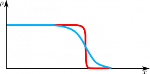
Both densities vanish at the material surface into the vacuum, but the electron density does it slower.
This is due to the fact that electrons are much lighter than nuclei and their wave functions will extend further into the vacuum.
One can see that imbalance of the densities will form excess of positive charge just below the surface and excess of negative charge just outside of it. In other words, an electric dipole is formed.
The dipole generates an electric field in a thin layer surrounding the crystal. The electric field will point outwards the surface thus producing an electric potential barrier for the electrons crossing the surface.
In short, the surface dipole will prevent low energy electrons from escaping the material.
The height of the surface potential barrier will depend on the density of lattice sites on the surface. Thus, crystal faces that have more lattice sites per unit surface area will tend to show stronger repulsion towards carriers from the bulk.
Although the width of the dipole layer (i.e., the width of electron charge density tail) is very small and does not exceed the lattice constant of the crystal, the resulting potential barrier is macroscopic and extends into the vacuum like $\propto d^{-2}$, where $d$ is the distance from the surface.
Work function for positive dipole
The graph below depicts an electric potential experienced by an electron on its path to freedom.
In the bulk, electrons have energies of up to Fermi level $E_F$.
In vacuum, the lowest energy state has energy $E_{vac}$. If a single electron is brought from the vacuum to the bulk,
the energy $|\mu|$ would be released. This is, by definition, a chemical potential $\mu$. $\mu$ is negative if the energy is released when moving an electron from infinity to the bulk of the material and positive if the energy needs to be delivered.
The surface dipole manifests itself in the surface dipole potential $V_{sdp}$.
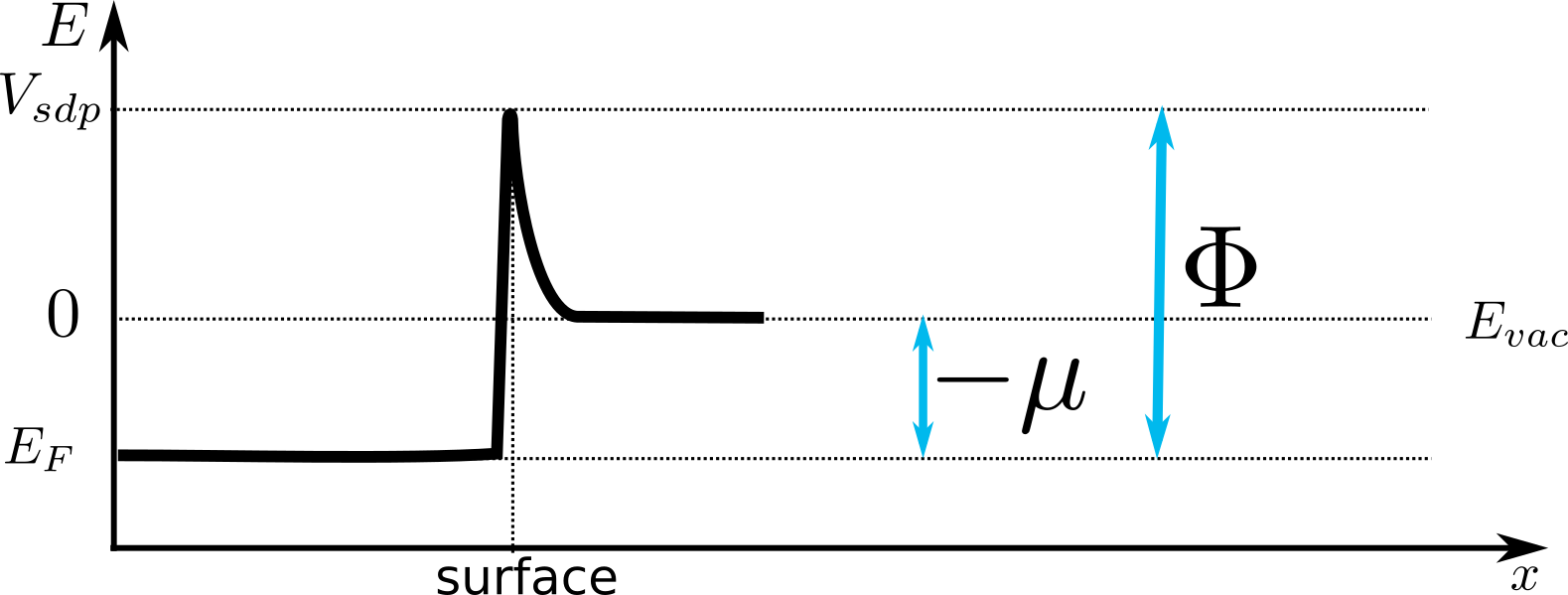
An electron in the bulk of the material would need to gain at least
$$\Phi=-\mu + V_{sdp}$$
of energy in order to escape to vacuum. And this is the work function.
A word of caution
The potential plotted above is one-dimensional. It is so, because electron’s trajectory is one-dimensional.
It is important to keep in mind that the trajectory is submerged in a three-dimensional space. Only 3D electric fields can produce such a potential from the surface dipole on a finite surface. A 1D dipole can generate only a step-function potential. That means that in 1D world, the surface dipole potential does not decay to zero with the growing distance from the dipole and $ \Phi=-\mu$ .
Work function for negative dipole
The positive dipole due to the different tunneling capabilities of positive and negative charges raised the energy barrier for electrons at the surface. It is also possible to engineer metal surface with a negative surface dipole.
One mechanism is discussed in the R. Smoluchowski article.
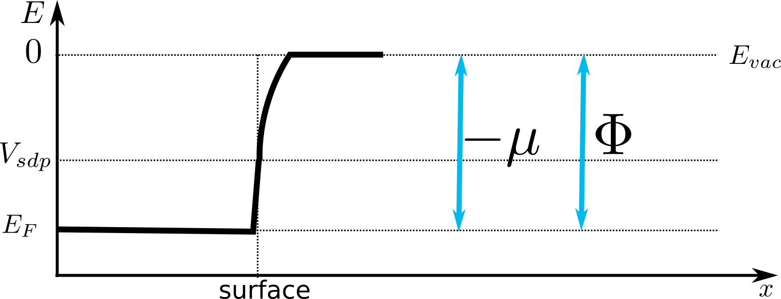
In the case the surface dipole potential is negative or zero, the numerical value of the work function is given by
$$
\Phi = -\mu.
$$
Here the work function is actually equal to the difference between the lowest vacuum level and the Fermi level.
Image charge
The dipole layer consideration above tacitly assumes, as is common in electrostatics, that an electron is a test charge, i.e., the infinitesimally small negative charge that does not affect other charges and thus the electric potentials it experiences$^*$.
Since the work function is the work done on an electron and not on a test charge, the assumption needs to be revised.
Indeed, an electron leaving the material will interact with all other charges in such a way that as soon as it crosses the surface it will induce an image charge on the side of the material. The mobile charges (carriers) on the material surface will adjust their positions to create electric potential as if there was a positive “electron” inside the material. The distance of the mirror charge from the flat surface will be equal to the distance of the electron from the surface.
Because of the image charge is positive, the electron is attracted to it and some work needs to be applied to overcome that attraction.
The force between the two charges at distance $2d$ is given by the Coulomb’s law
$$
F = - \frac{1}{4\pi\varepsilon_0} \frac{qq’}{4d^2},
$$
where the minus sign indicates that the force acting on an electron pulls it back to the surface.
One can imagine that the electron moves in a fictitious electric potential
$$
\phi_{img} = \frac{1}{4\pi\varepsilon_0}\frac{q’}{2d}.
$$
The potential is fictitious because a test charge would not be affected by it.
Anyway, the image charge potential decreases with increasing distance from the surface like $d^{-1}$, i.e., slower than the potential of a dipole layer. Also, it is always attractive.
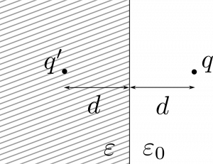
In general, the charge $q$ outside a material with permittivity $\varepsilon$ will induce an image charge $q’$ such that
$$
q’ = \frac{\varepsilon_0 - \varepsilon}{\varepsilon_0 + \varepsilon}q,
$$
where $\varepsilon_0$ is vacuum permittivity.
For metals, $\varepsilon \to \infty^{**}$ and $q’ = -q$.
For semiconductors and dielectrics, where $\varepsilon > \varepsilon_0$, the $q’ $ will still have opposite sign to $q$ but smaller magnitude. Thus, the image charge attraction will be less pronounced.
Finally, the energy potential the electron is subjected to, due to the image charge effect, is given by
$$
V_{img} = -\frac{1}{8\pi \varepsilon_0}\frac{1}{d}\frac{\varepsilon_0-\varepsilon}{\varepsilon_0+\varepsilon}e,
$$
where $e$ is a positive elementary charge.
Helmholtz and Langmuir p. 200-207 claim that this image charge potential is the dominant component of the work function of metals.
Notice, that the effect will also depend on the surface density (crystallographic orientation) of material atoms.
$^*$ A similar distinction holds for definitions of voltage and electromotive force. The voltage corresponds to the work performed on a test charge when moving between two locations in an electric potential while electromotive force is the work done on an electron.
$^{**}$ To be more precise, for metals the imaginary part of the permittivity is infinite or can be treated as such. The real part is the same as for vacuum, i.e.: $\varepsilon_0$.