CPD and monochromatic light
Although the interpretation of Contact Potential Difference (CPD) measurements is usually a difficult task because it involves variety of effects like
- sample inhomogeneity,
- surface roughness,
- surface dipole effects,
- light induced surface reconstruction,
- surface embedded impurities,
- sample thickness,
- back contact properties
- and many more,
it is important to have an understanding of basic Surface Photovoltage mechanisms.
In this answer I will use nomenclature from L. Kronik, Y. Shapira / Surface Science Reports 37 (1999) 1:206.
Photons with energy higher than bandgap will be called super-bandgap photons and those with lower energy: sub-bandgap photons.
Assumptions
Here is the list of assumptions made in what follows:
- sample is homogeneous with no surface roughness
- it is thick enough, so that light does not interact with the carries on the back contact interface
- there are no surface impurities
- there no trap states,
- the only states with energies in the gap are the surface states
- there are no molecules adsorbed at the surface
- work function of the sample is smaller than the work function of gold (tip)
- light intensity is large enough to lower the surface potential with super-bandgap photons.
I will also, unlike Kronik and Shapira, avoid using a misleading term of “band bending” which should be best abandoned altogether.
Sub-bandgap photons
N-type semiconductor

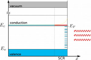
Here is the energy diagram for n-type semiconductor. It has some surface states in the energy gap.
They are mostly occupied by electrons, up to the Fermi level [imath]E_F[/imath]. The yellow line represents an energy potential function for electrons. Negative carriers, i.e., mobile electrons in conduction band, are repelled from the surface by trapped surface charges and the Space Charge Region is formed.
When low energy photons are shined upon the surface:
- they cannot excite a valence band electron to the conduction band because they don’t have enough energy
- they cannot excite a valence band electron to the surface state because the surface states are already occupied
- they can excite the surface electrons to the conduction band, where they will be immediately pushed to the bulk by potential in the SCR
- if the electrons are removed from the surface, it becomes less negatively charged
- if the surface is less negatively charged, it becomes more difficult to remove an electron from thus the work function increases and CPD increases or becomes less negative. For example, CPD will change from -100 mV to -50 mV.
P-type semiconductor

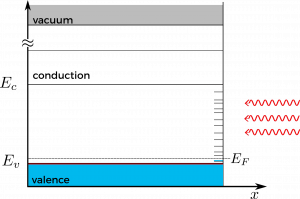
For p-type semiconductor the surface states in the energy gap will be mostly empty. The surface charge will be less negative than in the n-type semiconductor. That would indicate much lower sensitivity to light, because SCR will be smaller, too. For that reason SCR is not drawn in the diagram.
When low energy photons hit the semiconductor:
- they cannot excite an electron in valence band to the conduction band, because they have insufficient energy
- they cannot excite surface states to the conduction band for the surface states are empty,
- however, they can excite valence band electrons to the surface states
- thus, the surface will be charged negative
- work function will decrease, so the CPD will decrease. For example CPD will go from -100 mV to -200 mV.
Super-bandgap photons
N-type semiconductor

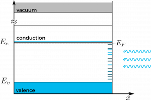
Here are the processes for super-bandgap photons:
- they have enough energy to excite valence band electrons to the conduction band
- both bands have much larger state density than surface states. That means that the inter-band excitation will be way more probable than band-surface excitation
- the valence band electrons excited to the conduction band will be numerous and they will destroy the Space Charge Region and the surface potential
- no surface potential will increase surface electron density hence work function will decrease and CPD will decrease. For example, CPD value could change from -100 mV to -200 mV.
P-type semiconductor

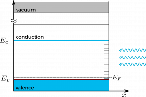
This scenario will involve the following analysis
- photons will couple the valence and the conduction band
- in comparison, the direct coupling with surface states can be neglected
- there will two processes removing conduction band electrons: recombination and deexcitation to the surface states
- recombiantion does not affect the surface charge density, deexciation does
- the deexciation will charge the surface negative
- if surface becomes negatively charged, the work function will decrease, so the CPD will decrease as well. For example, CPD could shift from -100 mV to -200 mV.
Summary
In the four cases considered CPD will increase only for low energy illumination of an n-type semiconductor.
Otherwise CPD decreases.