The request
During recent “Non-linear phenomena in electrochemistry and photovoltaics” conference Q&A session, dr. Bienkowski
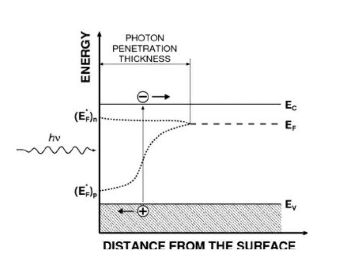
asked for explanation of the picture

from the Idris at al. publication.
That plot shows a type-n semiconductor energy band diagram with the Fermi level $E_F$ that splits at the surface
into two Quasi Fermi levels (QFLs):
$$
(E_F^*)_n
$$
for electrons and
$$
(E_F^*)_p
$$
for holes.
The QFLs arise because the semiconductor is driven out of equilibrium by the incident photons.
Both of the QFLs firmly sit in the energy gap between valence and conduction bands.
QFL definition/intuition
Lets confront that picture with the wikipedia definition of QFLs. The definition is inspired by similar in spirit explanations of QFLs in solid state textbooks. The brief definition states that:
A quasi Fermi level (also called imref, which is “fermi” spelled backwards) is a term used in quantum mechanics and especially in solid state physics for the Fermi level (chemical potential of electrons) that describes the population of electrons separately in the conduction band and valence band, when their populations are displaced from equilibrium. This displacement could be caused by the application of an external voltage, or by exposure to light of energy $E>E_g$, which alter the populations of electrons in the conduction band and valence band. Since recombination rate (the rate of equilibration between bands) tends to be much slower than the energy relaxation rate within each band, the conduction band and valence band can each have an individual population that is internally in equilibrium, even though the bands are not in equilibrium with respect to exchange of electrons. The displacement from equilibrium is such that the carrier populations can no longer be described by a single Fermi level, however it is possible to describe using concept of separate quasi-Fermi levels for each band.
Indeed, the intra-band relaxations for electrons and holes in conduction and valence band, respectively, are much faster
(order of ps) than the inter-band transitions (order of ns). Thus, it seems reasonable to assume that electrons within conduction band reach the equilibrium before any recombination process occurs. So, it follows, that the conduction band occupation of levels should obey its own Fermi-Dirac distribution. Similar for holes in the valence band.
The two Fermi-Dirac statistics give two Quasi Fermi levels, one in each band.
The problem
There is a grave mistake in that approach. As pointed out to me several years ago by prof. Kuncewicz, if the picture was correct then the QFL for electrons should be always above the $E_C$, the lowest energy of the conduction band.
This is because, the $E_C$ level is always “fully” occupied$^{*}$ since relaxed electrons will thermalize to the bottom of the conduction band.
Akin argument holds for the valence band. QFL for holes should always reside below the upper valence band edge $E_V$.
That is why the intuition behind the QFLs is incompatible with the picture shown above, and with the pictures presented in the same wikipedia article, BTW.
A possible way out
The intuition from the textbooks and from wikipedia makes no sense. A small perturbation should result in a small QFLs splitting. After all, a photocurrent generated by the perturbation is proportional to that splitting. The common “explanation” suggests the splitting always greater than the gap energy $E_g$.
We need a new intuition.
The way out of the problem may be offered by Landauer’s picture of electron transport. See the conscientious lecture by prof. Supriyo Datta on QFLs in nanoelectronics.
Both QFLs there describe occupation of left-moving electron states and right-moving electron states. As with an ordinary Fermi level, the QFLs separate the states mostly occupied from mostly empty.
The imbalance in the occupation results in a net current.
$^{*}$ This is incorrect. For nonzero temperatures and small light intensities the bottom of the conductance band is not fully occupied. See the Radim’s post and my follow up.